PSI researchers use extreme UV light to produce tiny structures for information technology
In many areas of information technology, the trend towards ever more compact microchips continues unabated. This is mainly because production processes make it possible to achieve ever smaller structures, so that the same number of information-processing components takes up less and less space. Fitting more components into less space increases the performance and lowers the price of the microchips used in smartphones, smartwatches, game consoles, televisions, Internet servers and industrial applications.
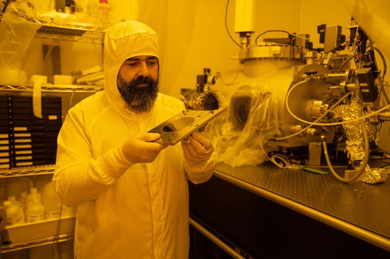
A research group led by Dimitrios Kazazis and Yasin Ekinci at the Laboratory for X-ray Nanoscience and Technologies at the Paul Scherrer Institute PSI, in collaboration with researchers from University College London (UCL) in the UK, has now succeeded in making important progress towards further miniaturisation in the IT industry. The scientists have demonstrated that photolithography – the method of patterning widely used in the mass production of microchips – works even when no photosensitive layer has been applied to the silicon.
Writing patterns in silicon
Photolithography, which literally means “drawing on stone with light”, is the most important process in the industrial manufacture of electronic components. In principle, it works like exposing a photographic film to light, except that the carrier material is silicon rather than celluloid. A light-sensitive material, technically known as a photoresist, is applied to a silicon wafer. This is exposed to light in the pattern of the blueprint for the chip, which alters the chemical properties of the photoresist. This either becomes firmer or less firm. Subsequent treatment removes the exposed (positive process) or the unexposed (negative process) areas, leaving behind the desired circuit pattern, including the conductive traces. At present, this process is mainly carried out using lasers with a wavelength of around 240 to 193 nanometres.
However, the PSI researchers took a different approach. They opted against a photoresist, which degrades the image and is therefore an obstacle to miniaturisation. Ekinci: “Photoresists are made of polymers. At the macro level they look smoother than a mirror, but at the atomic level they look like a tangle of wires.” For the exposure, they used extreme ultraviolet light, or EUV for short, from the Swiss Light Source SLS at PSI. The researchers were able to create structures, i.e. circuit traces, that were just 75 nanometres wide. By comparison, a human hair is about 930 times thicker. “These are the smallest structures ever written with photons without using a photosensitive coating,” Kazazis explained. The researchers describe their experiment as a “proof of principle”.
Smaller and smaller and smaller
EUV light plays a key role here. Exposure to these soft X-rays can on its own increase the sensitivity of the silicon to an etching solution or developer – if the wafer has been treated chemically beforehand. The researchers achieved this by treating the silicon with hydrofluoric acid.
The new process opens the door to further extreme miniaturisation steps. However, Kazazis warns against raising expectations too high, saying that it will be “decades” before the procedure can be used in a mass production setting – and it will require a lot of tinkering around. “Although there is still a lot of work to do before the technique is suitable for industrial integration, we are excited by its potential for high-resolution patterning and it points to many promising avenues for future research,” explains the PSI researcher. “Not only in terms of patterning classical devices, but also quantum devices.”
