Scientists now able to map defects in 2D crystals in liquid
Monolayer crystals, often being referred as 2D crystals or 2D materials, possess the unique characteristic of having a single layer of regular atomic structure. And the more regular the structure is, the higher quality the crystal. In some cases, the atomic structure is repeated to perfection, but most of the time – as is usually the case in nature – there are some flaws.
Molybdenum disulfide (MoS2), a black crystal that looks like graphite, is one example of a crystal that has such layered structure in which defects can be present. “The atoms in the monolayer MoS2 are arranged in three layers, like a sandwich – a bottom layer of sulfur atoms, and then a layer of metal atoms, and finally another layer of sulfur atoms,” says Aleksandra Radenovic, the head of the Laboratory of Nanoscale Biology at EPFL’s School of Engineering. “But sometimes, some sulfur atoms are missing, which leads to vacancy defects in the crystals. Such defects can also be beneficial. For example, they catalyse the water-splitting reaction to produce hydrogen or serve as target sites in detectors of biomolecules. This is why we are interested in these defects, especially in their behavior in liquid.”
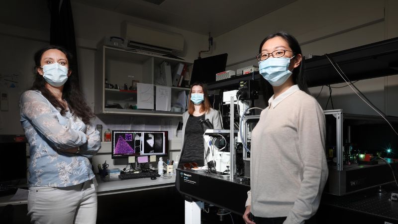
Radenovic, along with postdoc Miao Zhang, Martina Lihter, former PhD student, and collaborators, studied MoS2 samples and developed a method for mapping these kinds of defects in liquid, leading to a better understanding of the material’s properties. In electron microscopy, which allows direct visualisation of defects with superb resolution due to the use of high energy electron beam, vacuum environment is required. “Measurements in the liquid are still challenging”, says Radenovic. To be able to visualize the defects sites in liquid, LBEN team adapted the optical microscopy imaging modality termed Point Accumulation in Nanoscale Topography, PAINT. The work is recenltley published in ACS Nano.
Because the monolayer MoS2 crystal is only three layers of atoms thin, it is almost transparent, which allows the scientists to observe it through a thin glass coverslip on an inverted microscope. “We placed our sample in an aqueous solution to study the defects’ activity in the liquid environment,” says Lihter.
The scientists then used fluorescent thiol probes that bind specifically to the sulfur vacancies. “By directing a laser beam on the sample, we are able to directly see a single probe which bound to a defect and precisely locate its position,” says Zhang. It turns out that such binding is reversible under certain conditions. By imaging such random transient binding at defects over a period of time, as an reminiscence of the PAINT strategy, the scientists were able to identify and count the crystal’s defects and quantify its imperfections, all at a relatively large scale. “In this way, we could also observe how the defects interacted with their environment,” says Zhang.
Altering a material’s properties
The sulfur vacancies have the result of changing the material’s properties. MoS2 is a semiconducting material used to make chips for electronic devices. The experiments conducted by Radenovic’s team were therefore intended not just to map defects, but also to study the material’s behavior to heal the defects. “An irregular atomic structure modifies the way electrons move inside a material and the material’s carrier mobility,” says Radenovic. “That consequently alters its properties.”
While the scientists focused on MoS2 for this study, their method is applicable to other materials in the same family (transition metal dichalcogenide) that have a sandwich atomic structure.
