A transistor from the printer
At first glance, it sounds like a contradiction: printed electronics, such as transistors, electronic semiconductor components for controlling voltages and currents, which can be applied to any substrate by a printer. Can such a thing really exist? Absolutely! The world is eagerly awaiting such innovations, especially for the fast-growing Internet of Things, which has billions, even trillions, of interconnected sensors and devices. In order to produce such huge amounts, fast printing processes must be developed using roll-to-roll processing on flexible substrates such as polymers or paper.
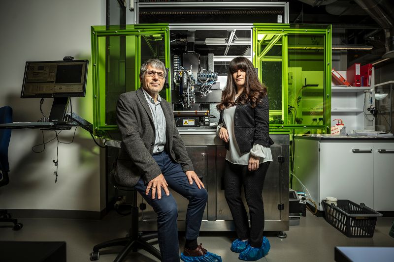
Printed electronics is an extremely multidisciplinary field. Jakob Heier, for example, is a physicist, has a doctorate in materials science and engineering, worked for a time at a start-up on the development of electronic paper, and became involved in the formulation of inks and printing via polymer physics. In addition to leading his research group at the Empa Laboratory for Functional Polymers, he is currently also responsible for servicing the pressure systems required for printing electronics at the Coating Competence Center (CCC).
Evgeniia Gilshtein, for her part, is a postdoc at the Empa Laboratory for Thin Films and Photovoltaics. A team from this laboratory had some time ago succeeded in printing electronic circuits and sensors from anorganic materials on polymer films. This breakthrough was made possible thanks to the “FOXIP” (Functional Oxides Printed on Polymers and Paper) project, which was financed by the ETH Domain’s strategic research priority “Advanced Manufacturing”. While it has been known for a long time how to print organic transistors, the Empa team, together with colleagues from EPFL and the PSI, attempted for the first time to print inorganic transistors, which not only promise higher performance, but are also significantly more stable. Inks made of oxide nanoparticles were used in this process. These are conductive inks that are transformed into printed electronics using highly specialised facilities in Empa’s CCC. The tolerances during printing are within the micrometer range.
“The foreseeable need for printed electronics is huge,” is how Heier assesses the situation, adding that “the more often thin sensors are also used to monitor physical conditions or on food packaging and other applications, the greater the demand will be.” In 2020, a relevant report showed that this sector has now developed into a global market of more than 35 billion dollars a year. And the trend is set to continue strongly. A novel application of printed electronics for which Gilshtein is responsible is almost prototypically associated with this development.
Invisible keypad
Using printed electronics, the Empa researcher has developed an invisible keypad where only authorised persons know how and where to enter the access code – the perfect camouflage for doors, lockers or even windows. Gilshtein was able to build on Empa’s existing know-how relating to the printing of electronics on thin-film foils and to further develop this in a sophisticated way. First, the capacitive sensors were printed on the carrier foil, as has been done many times. Then, however, it was necessary to make the metal indium tin oxide-based nanoparticle ink more transparent and conductive than conventional substances. This was done using a trick: the patterns already printed on foils were dyed blue and “processed in a millisecond with a super-bright, energy-rich light source,” said Gilshtein, adding that “the dye completely absorbs the incident light in the nanoparticles layer and makes it a homogeneous solid layer.”
And as a certainly desired side effect, the blue dye decomposes during this process, and the electrically conductive indium tin oxide layer becomes optically transparent, i.e. invisible to the human eye.
The “secret ink” developed in this way is what made an invisible keypad for a safe possible in the first place. “Flash lamp annealing is the actual breakthrough. This means that we reach in exactly the right location in the blink of an eye, namely in the printed layer the required temperature of more than 500°C, in order to produce the electrically conductive material. The surface to be printed, i.e. paper or polymers, is hardly heated during this process,” said Gilshtein.
However, the Empa researcher now wants to turn her attention to another scientific topic: stretchable printed electronics, ultra-thin sensors which will be applied directly to the human skin in a variety of forms. “Is this set to be the next big thing in printed electronics?”
